- 您现在的位置:买卖IC网 > Sheet目录223 > ESD0P8RFL E6327 (Infineon Technologies)DIODE ESD 12V DUAL TSLP-4
ESD0P8RFL
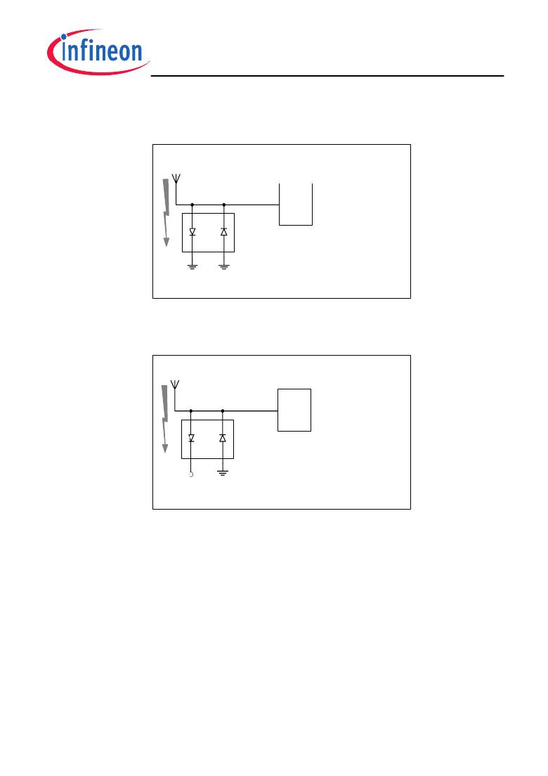
1. Application example
1 RF signal channel, anti-parallel configuration,
please refer also to Application Note No.103
1 protected signal line,
superimposed DC voltage up to
±V F (diode forward volatge)
I/O
ESD
sensitive
circuit
The protection diode should be
placed very close to the location
where the ESD or other transients
can occur to keep loops and
inductances as small as possible.
Grounded pins should be
connected in parallel directly to a
Line to ground capacitance
0.8 pF @1 GHz
2. Application example
1 RF signal channel, rail-to-rail configuration
1 protected signal line,
ground plane on the board.
superimposed DC voltage up to
+Vcc (voltage supply)
I/O
ESD
sensitive
circuit
Cathode of one diode should be
connected to the positive supply
voltage +Vcc and anode of the
opposite diode should be
connected directly to a ground
plane on the board. Clamped
+Vcc
Line to ground capacitance
0.8 pF @1 GHz
5
input voltage at I/O port is limited
to Vcc + VF at positive transients
and 0V - VF at negative transients
(VF ... diode forward voltage
drop).
2011-06-27
发布紧急采购,3分钟左右您将得到回复。
相关PDF资料
ESD1014MUTAG
IC TVS ARRAY LOW CAP 10UDFN
ESD11A5.0DT5G
TVS UNIDIR 150MW 5.0V SOT-1123
ESD11B5.0ST5G
TVS BIDIR 250MW 5V DSN2
ESD11L5.0DT5G
TVS ESD UNIDIRECT 150MW SOT-1123
ESD11N5.0ST5G
TVS BIDIR 250MW 5V DSN2
ESD1P0RFWE6327
DIODE RF ESD 1CH SOT323
ESD3V3U1U-02LS E6327
DIODE TVS 3.3V TSSLP-2-1
ESD3V3U4ULC E6327
DIODE TVS 3.3V TSLP-9-1
相关代理商/技术参数
ESD0P8RFLE6327
制造商:Infineon Technologies AG 功能描述:
ESD0P8RFLE6327XTSA1
制造商:Infineon Technologies AG 功能描述:ESD Suppressor Diode Arrays 20KV 4-Pin TSLP T/R 制造商:Infineon Technologies AG 功能描述:TVS DIODES - Tape and Reel 制造商:Infineon Technologies AG 功能描述:DIODE ESD 12V DUAL TSLP-4
ESD10
功能描述:保险丝 10A 550VAC IND
RoHS:否 制造商:Littelfuse 产品:Surface Mount Fuses 电流额定值:0.5 A 电压额定值:600 V 保险丝类型:Fast Acting 保险丝大小/组:Nano 尺寸:12.1 mm L x 4.5 mm W 安装风格: 端接类型:SMD/SMT 系列:485
ESD1000
制造商:未知厂家 制造商全称:未知厂家 功能描述:OEM Bluetooth-Serial Module
ESD1000SK
制造商:未知厂家 制造商全称:未知厂家 功能描述:OEM Bluetooth-Serial Module
ESD100121
制造商:Panasonic Industrial Company 功能描述:SWITCH
ESD100121AQ
制造商:Panasonic Industrial Company 功能描述:SWITCH
ESD100124
制造商:Panasonic Industrial Company 功能描述:SWITCH
